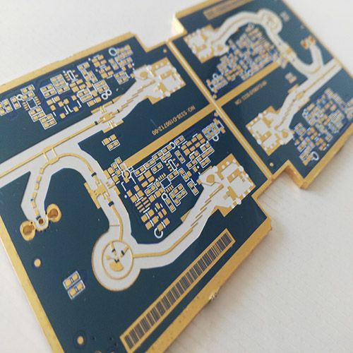
What is the High Frequency PCB
High Frequency PCB may be a quite PCB, which is widely used for special signal transmission between objects. It operates from 500MHz to 2GHz and is right for mobile, microwave, RF and high-speed design applications.
Publié le December 12,2020 dans la catérogie Economie et Commerce.
High Frequency PCB may be a quite PCB, which is widely used for special signal transmission between objects. It operates from 500MHz to 2GHz and is right for mobile, microwave, RF and high-speed design applications. With the increasing complexity of electronic components and switches, faster signal flow and better transmission frequency are needed. High Frequency PCB PCB can play a really important role.Due to the short rise time of the pulse in electronic components, it is necessary to consider the conductor width as an electronic component in HF technology.
Depending on the parameters, the HF signal is reflected on the circuit board, which means that the impedance (dynamic resistance) changes relative to the transmitting component. To avoid such capacitive effects, all parameters must be specified accurately and implemented with the highest level of process control.
For the impedance of high frequency circuit board, the key is the geometry of the conductor, the stacking of layers and the dielectric constant (ε R) of the materials used. Alcanta PCB provides you with know-how, all common materials and qualified manufacturing processes – reliable even for complex requirements.
High frequency PCB is a kind of PCB used for signal transmission in a variety of applications, including mobile, microwave, RF and high-speed design applications. High frequency boards with high frequency laminates are difficult to manufacture because they need to maintain the heat transfer of the application due to the sensitivity of the signal.
Function of high frequency PCB
- DF should be very small, which mainly affects the quality of signal transmission. The smaller the DF, the smaller the signal loss.
- The coefficient of thermal expansion should be the same as that of copper foil as much as possible, because this difference will lead to the separation of copper foil in cold and hot changes.
- Water absorption must be low. In humid environment, high water absorption will affect DK and DF.
- Heat resistance, chemical resistance, impact resistance and peel resistance must be good.ww.tapatalk.com/groups/tapatalksupport/aluminum-pcb-t45849.html
Manufacturing high frequency board
According to Rush PCB, all of the above laminates have individual manufacturing problems. In order to obtain the required quality and reliability, the corresponding manufacturing instructions for each material need to be followed for processing, storage, surface treatment, inner layer treatment, drilling, bonding, deburring and electroplating.
Special process is needed to make PCB with HF material. For example, preparation of plated through holes is a critical process, especially for PTFE substrates. The surface of the PTFE is specially prepared to receive the etching process. Therefore, with the correct selection of materials, following the appropriate manufacturing method is also essential for obtaining high-quality plates and working at high frequencies.
Before selecting high frequency PCB and materials suitable for your project, you must consider the following points:
Dielectric constant is the ability of a material to store energy in an electric field. It depends on the direction of the material, that is, it will change with the material axis. It must be small enough to provide a stable input to avoid any delay in the transmitted signal.
Similarly, high DF will seriously affect the quality of the transmitted signal, so the loss factor must be very small. Therefore, the less DF, the less signal waste.
Loss tangent is another factor based on the molecular structure of the material, which can affect RF materials containing high frequencies. However, for low frequency signals, it is not very important.
In terms of crosstalk and skin effect, proper spacing is very important. Crosstalk occurs when boards begin to interact with themselves and are associated with unwanted coupling of their own components. In order to avoid crosstalk, the distance between the line and the plane must be minimized.
Skineeffect is directly related to the resistance of the wiring. As the resistance increases, it begins to increase, eventually causing the board to heat up. Therefore, the length of the circuit board must be selected in a higher frequency manner.
Different manufacturers offer a wide range of materials for high frequency applications.
- UL certified, flammability V-0, IPC-TM-650 compliant
- Low loss factor, DF = 0.0018 at 1.9 GHz
- Excellent peel strength, greater than 10 lb / in
- 3.5 at low dielectric constant DK = 1.9 GHz
- Low moisture absorption less than 0.02%
- The CTE of the z-axis is as low as 64 ppm / ° C
For more information, please click:PCB Fabrication