Heavy copper pcb - PCB Manufacturer-ALCANTAPCB
Heavy copper pcb and extreme copper pcb are getting used by more and more power electronic products. Most commercial PCBs are manufactured for low voltage / low power applications, with copper weights starting from 1 / 2 oz / ft2 to three oz / ft2 for copper routing / planar applications.
Posted December 12,2020 in Other.
Heavy copper pcb and extreme copper pcb are getting used by more and more power electronic products. Most commercial PCBs are manufactured for low voltage / low power applications, with copper weights starting from 1 / 2 oz / ft2 to three oz / ft2 for copper routing / planar applications. Heavy copper pcbs are manufactured with copper weights between 4 oz / ft2 and 20 oz / ft2. Copper weighing quite 20 oz / ft2 to up to 200 oz / ft2 is additionally possible, referred to as extreme copper. Our discussion will focus mainly on heavy copper.
The construction of heavy copper pcb makes the circuit board have the following advantages:
- It increases the bearing capacity of thermal stress.
- The current carrying capacity increases.
- The position of the connector and the mechanical strength in the PTH hole are improved.
- In the case of no circuit failure, make full use of exotic materials to achieve their full potential (i.e. high temperature).
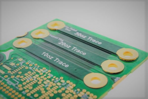
- The product size is reduced by combining multiple copper weights on the same circuit layer (see Figure 1).
- Heavy copper plated vias flow higher current through the plate and help transfer heat to the external radiator.
- The on-board radiator is directly plated onto the plate surface using up to 120 ounces of copper.
- On board high power density planar transformer
Heavy copper PCB function
Pcbogo is an experienced person, PCB manufacturer can develop and produce outstanding high quality heavy copper PCB products. We can provide heavy copper PCB manufacturing services, using up to 13 ounces of copper. Please check the functions in the table below:

Application of heavy copper PCB
Needless to say, heavy copper PCB has been widely used in various electronic industries, such as heat dissipation, high power distribution, planar transformer and power converter. What’s more, there is a great demand for heavy copper PCB in computer, automobile, military and industrial control.
In addition, heavy copper PCB board is also used for other purposes:
- Power supply, power converter
- Automobile industry
- Welding equipment
- Power distribution
- Power line monitor
- Torque control
- Overload relay
- Protection relay
- Solar panel manufacturers, etc.
Construction of heavy copper pcb
Standard printed circit boards, whether double-sided or multilayer, are manufactured by a combination of copper etching and electroplating processes. The circuit layer starts with a thin copper foil (usually 0.5 oz / ft2 to 2 oz / ft2), then etched to remove excess copper, and then plated to increase the copper thickness for flat, wire, pad, and plated through holes. All circuits are laminated into a complete package using an epoxy based substrate such as FR4 or polyimide.
Boards containing heavy copper pcbs are produced in exactly the same way, despite the use of specialized etching and electroplating techniques such as high-speed / step plating and differential etching. Historically, heavy copper features have been formed entirely by etching thick copper clad laminate materials, resulting in uneven routing sidewalls and unacceptable undercutting. Advances in electroplating technology have allowed the combination of electroplating and etching to form heavy copper features, resulting in straight sidewalls and negligible undercuts.
Electroplating of heavy copper pcbs enables plate manufacturers to increase the copper thickness in the plating holes and through-hole sidewalls. Heavy copper with standard features can now be mixed on a single board (also known as PowerPoint). Advantages include reduced number of layers, low impedance power distribution, smaller footprint and potential cost savings. Generally, high current / high power circuits and their control circuits are produced separately on separate boards. A large number of copper plating can integrate high current circuit and control circuit, so as to realize high density and simple circuit board structure.
Heavy copper pcb strength and survivability
Circuit board manufacturers and designers can choose from a wide range of dielectric materials, from standard FR4 (operating temperature 130 ° C) to high temperature polyimide (operating temperature 250 ° C). Exotic materials may be required for high temperature or extreme environmental conditions, but will they survive in extreme conditions if the standard setting for circuit routing and via plating is set to 1 oz / ft2? The circuit board industry has developed a test method for determining the thermal integrity of finished circuit products. The thermal strain comes from the manufacturing, assembly and maintenance processes of various circuit boards. The difference of CTE between copper and PWB laminates provides a driving force for the development of crack nucleation and circuit failure. The thermal cycle test (TCT) checks whether the resistance of the circuit increases when air to air thermal cycling from 25 ° C to 260 ° C occurs.
An increase in resistance indicates a decrease in electrical integrity due to cracks in the copper circuit. The standard sample design for this test uses 32 plated through-hole chains, which has long been considered to be the weakest point of the circuit under thermal stress.
TCT results clearly show that the failure rate becomes unacceptable no matter what kind of plate is used. Thermal cycling studies on standard FR4 boards with 0.8 to 1.2 mil copper plating showed that 32% of the circuits failed after eight cycles (a 20% increase in resistance was considered a failure). Printed circuit boards with heterogeneous materials show a significant increase in this failure rate (up to 3% after eight cycles for cyanates), but the price is too high (five times 10 times the material cost) and difficult to process. A typical SMT component has to go through at least four thermal cycles before leaving the factory, and each component repair may require another two thermal cycles.
The use of heavy copper pcbs will completely reduce or eliminate these faults. Plating 2 oz / ft 2 copper on the hole wall can reduce the failure rate to almost zero (TCT results show that for standard FR4, after eight cycles, the coating is at least 250 mils with a failure rate of 0.57%). In fact, the copper circuit becomes unaffected by the mechanical stress applied to it by thermal cycling.
For more information, please click:PCB Fabrication